 |
|
Michelle Te, I-Connect007 |
|
My husband and I recently became empty-nesters (again), and it’s an interesting dynamic when you aren’t arranging your daily routines around your kids’ schedules and lives. You don’t feel as rushed, and you can turn your attention to some other things that have been put on hold, but you also feel a little melancholy about the changes, and you hope you’ve instilled enough of your wisdom into your children before they move away.
More >
|
|
 |
|
Leo Lambert, EPTAC |
|
I spent a week in Paris in September at the IPC Builds meetings, and it gave me the chance to see, take part in, and document a broad range of technical and training-related discussions affecting the electronics manufacturing industry. I go to these meetings because what gets decided in those rooms ends up in the classes we teach at EPTAC. In addition to attending committee meetings, I participated in keeping minutes for several sessions because some meeting leaders were unable to attend due to travel restrictions.
More >
|
|
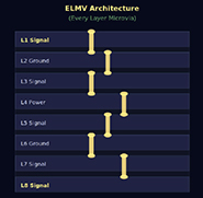
ELIC: Every Layer Interconnect - The Promise, the Pain, and the Practical Limits - As component pitches shrink and routing density climbs, ELIC is pushing PCB fabrication into territory closer to semiconductor packaging than traditional HDI. This whitepaper explores ELIC's density advantages, manufacturing challenges, DFM pitfalls, yield considerations, and why designing to a fabricator's real process window is critical to successful production. Download now. |
|
 Sponsored |
|
 |
|
Sukanya Natarajan, Global Electronics Association |
|
In July 2026, the Union Cabinet chaired by the Prime Minister approved the Semicon 2.0 for the development of India's semiconductor design and manufacturing ecosystem, with a total budget outlay of Rs. 1,27,500 crore (approximately 13.3 billion USD). With this, India could account for nearly 10% of the global semiconductor industry market in the coming years and is expected to play a much bigger role in the global semiconductor value chain, Union Minister for Electronics and Information Technology Ashwini Vaishnaw said while addressing a press briefing in New Delhi on Oct. 5.
More >
|
|
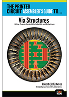
Will Your Vias Survive the Heat?
The Printed Circuit Assembler's Guide to... Via Structures: Reflow Process Survivability, Reliability, and Robustness, the latest book from I-Connect007’s respected technical library, challenges long-held assumptions about how the electronics industry evaluates PCB via structures. Drawing on decades of experience, author Bob Neves combines technical depth with practical guidance, providing engineers and manufacturers with a roadmap for evaluating today's increasingly complex via structures with greater accuracy and confidence. Download your free copy today. |
|
 |
|
| |
| EIN - Electronics Industry News Highlights |
|
| |
| Industry Resource Center - Technical Content |
|
|
|
| |
| JobCONNECT007 Featured Listings |
|
|
 |
Director of Product Management & Technology–Asia
SCHMOLL ASIA PACIFIC, an international machinery company serving the electronics industry (approx...
Apply Now
|
|
|
 |
Solutions Consultant – Americas
We are seeking a Solutions Consultant to provide technical expertise and pre-sales support to customers across North and South America...
Apply Now
|
|
|
| |
| MAGAZINES007 - Latest Issues |
|
I-Connect007
|
|
Global Electronics Association
|
|
SMTA
|
|
|
| |
| If this mailing was forwarded to you, subscribe here for your own copy of the Daily Newsletter. |
All rights reserved. \u00a9 2026 I-CONNECT007.com
Mailing address: IPC Publishing Group Inc., 3000 Lakeside Drive, Suite 105N, Bannockburn, IL 60015 |
I-Connect007 invites you to forward this newsletter to colleagues or associates who might be interested in our newsletters.
%BASIC:EMAIL% unsubscribing to this newsletter is easy, just click this link: Unsubscribe Here
Keep our newsletters coming: add "newsletter@iconnect007mail.com" to your address book / safe list.
|
|
|
|